

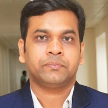
Md Arifuzzaman
PhD Researcher, Semiconductor & Graphene Device Process Engineering
Campbell,ACT
Work Preference
Summary
Semiconductor Device Engineer specialising in defect analysis in graphene, graphene device microfabrication, semiconductor process development and electrical characterisation. Extensive hands-on experience fabricating graphene field-effect transistor (GFET) devices through cleanroom manufacturing workflows, including CVD graphene transfer, photolithography, plasma etching, metal deposition, lift-off, ion implantation and electronic transport and gas sensing characterisation of GFET devices. Proven ability to optimise fabrication processes, investigate device failures and translate nanoscale materials engineering into high-performance electronic devices. Passionate about advancing graphene technologies from research into scalable semiconductor manufacturing.
Overview
4
4
Microfabrication, Defect Analysis, Electrical Characterisation,
7
7
Yeras of Teaching Experience in Tertiary Level
2
2
Languages
1
1
Certificate
Work History
PhD Candidate and Researcher
Australian National University
Canberra, Australian Capital Territory
03.2022 - Current
- Semiconductor Device Fabrication
- Independently fabricated 20+ batches of graphene field-effect transistor devices using semiconductor cleanroom processes.
- Manufactured 700+ graphene devices incorporating reproducible graphene transfer, lithography, plasma etching, metallisation and lift-off.
- Optimised fabrication workflows to improve device yield, reproducibility and electrical consistency.
- Developed multi-level lithography processes with accurate alignment for micro-scale graphene device fabrication.
- Deposited Cr/Au contacts using electron-beam evaporation and optimised lift-off processes for high-quality metal contacts.
- Process Development
- Designed semiconductor fabrication recipes for reproducible graphene device manufacturing.
- Performed process troubleshooting and optimisation across multiple fabrication stages.
- Improved fabrication repeatability through systematic process control and electrical verification.
- Materials Engineering
- Engineered graphene defects using controlled 30 keV carbon ion implantation.
- Quantified defect evolution through Raman spectroscopy and correlated defect density with electrical transport.
- Electrical Characterisation
- Characterised GFET devices using Agilent B1500A semiconductor analyser.
- Performed vacuum electrical measurements using Lakeshore temperature-controlled probe station from cryogenic temperatures to elevated temperatures.
- Extracted carrier mobility, contact resistance and Dirac voltage for process evaluation.
- Investigated device reliability through thermal annealing and temperature-dependent electrical measurements.
- Device Performance
- Developed defective graphene sensors exhibiting over five-fold improvement in NO2 responsivity compared with pristine graphene.
- Demonstrated reliable NO₂ detection down to approximately 10 ppb.
- Established relationships between fabrication processes, defect engineering and device performance.
- Engineering Achievements
- Defect engineering in graphene via low energy ion implantation and analysed through Raman spectroscopy
- Designed complete fabrication workflow for graphene FET devices.
- Fabricated 300+ semiconductor devices.
- Achieved reproducible cleanroom processing across 10+ fabrication batches.
- Demonstrated 10.65× enhancement in low-concentration NO₂ detection.
- Achieved ~10 ppb NO₂ limit of detection.
- Developed reproducible ion implantation methodology for graphene defect engineering.
- Elecltrical transport characterisation of GFET devices under vacuum and temperature controlled environment.
Senior Lecturer in Physics
North South University, Bangladesh
Dhaka, Bangladesh
09.2018 - 02.2022
Key Responsibilities & Achievements
- Delivered lectures and sessional classes, developing and updating syllabi in mechanics, solid-state physics and electromagnetism to enhance student learning.
- Published more than 10 peer-reviewed articles on magnetic nanoparticles, perovskite and two-dimensional materials.
- Provided technical mentoring and operational oversight, ensuring protocol compliance and data integrity while fostering collaboration among students and staff.
- Designed and set up experimental physics laboratories, establishing procedures, safety protocols and reproducible workflows.
- Led multidisciplinary nanomaterials research projects from concept through experimental validation, supervising student researchers while managing a competitive BDT 500,000 institutional grant. Developed reproducible experimental workflows, maintained comprehensive technical documentation and timely project delivery.
Teaching and Research Assistant
University of Lethbridge, AB, Canada
Lethbridge, Alberta, Canada
01.2015 - 08.2018
- Conducted spectroscopic research on atmospheric methane, analysing high-resolution FTIR spectra of methane mixing with air and methane itself to advance understanding of remote sensing of exoplanetary and Titan's atmosphere.
- Completed advanced courses on Molecular Spectroscopy.
- Collaborated with JPL, NASA to record high-resolution methane-air spectra, contributing to enhanced line profile and pressure induced shift coefficients of Metahne-air for correction of line profile data in public database such as GEISA nd HITRAN.
- Supported Physics sessional classes and marking scripts and assignments for undergraduate students as a Teaching Assistant across 6 roles.
Lecturer in Physics
International Islamic University Chittagong, Bangladesh
Chittagong, Bangladesh
02.2009 - 12.2016
Key Responsibilities & Achievements
- Developed and implemented physics curricula and sessional manuals laboratories for engineering programs.
- Established and maintained experimental physics laboratories with standardised procedures and safety protocols, ensuring safe and effective learning environments.
- Organised technical workshops and engineering activities as executive member of EEE Club, fostering hands-on skills and collaboration among participants.
Education
Ph.D. - Electronic Materials Engineering
The Australian National University
Canberra 04.2001 -
MSc - Physics
University of Lethbridge
Canada01-2017
M.Phil. - Physics
Chittagong Univ of Sci & Tech
Chittagong, Bangladesh12-2015
BSc (Hon’s) and M.Sc. - Physics
Shahjalal Uni of Sci & Tech
Bangladesh01-2008
Skills
Graphene transfer (CVD and mechanical exfoliation)
Direct-write photolithography
Mask aligner (SUSS-MA6)
Electron-beam lithography (EBL)
Microdevice fabrication (Two-layer lithography and mask alignment)
ICP-RIE and oxygen plasma etching
Electron-beam and thermal evaporation
Resist spin coating
Ellipsometry
Wafer scribing and cleaving
Metal lift-off processing
Defect engineering using ion implantation
Thermal annealing of graphene (Isochronal and Isothermal)
Semiconductor process optimisation
Raman spectroscopy
SEM, AFM, Optical microscopy & FTIR
Two-probe and four-probe electrical measurements
Gas sensing characterisation
Mass flow controller operation
Device optimisation & reliability evaluation
Documentation and reporting
Scientific writing
Experiment design
Research grants
Teamwork and collaboration
Timeline
PhD Candidate and Researcher
Australian National University
03.2022 - Current
Senior Lecturer in Physics at North South University, Dhaka, Bangladesh
09-2018
Senior Lecturer in Physics
North South University, Bangladesh
09.2018 - 02.2022
Teaching and Research Assistant
University of Lethbridge, AB, Canada
01.2015 - 08.2018
Lecturer in Physics
International Islamic University Chittagong, Bangladesh
02.2009 - 12.2016
Ph.D. - Electronic Materials Engineering
The Australian National University
04.2001 -
MSc - Physics
University of Lethbridge
M.Phil. - Physics
Chittagong Univ of Sci & Tech
BSc (Hon’s) and M.Sc. - Physics
Shahjalal Uni of Sci & Tech
Work Availability
monday
tuesday
wednesday
thursday
friday
saturday
sunday
morning
afternoon
evening
swipe to browse
Quote
"Nature isn't classical, dammit, and if you want to make a simulation of nature, you'd better make it quantum mechanical, and by golly it's a wonderful problem, because it doesn't look so easy."
Richard P. Feynman (1981)
Accomplishments
- Fabricated graphene field-effect transistor (GFET) devices through end-to-end semiconductor cleanroom processing, from CVD graphene transfer to electrical characterisation.
- Developed controlled defect engineering of graphene using 30 keV ion implantation, enabling 10.65× higher NO₂ sensitivity at 0.1 ppm and ~10 ppb detection capability.
- Led gas sensing experiments in collaboration with RMIT University, demonstrating high-performance defective graphene sensors through systematic device testing and data analysis.
- Secured and managed competitive research funding, including a BDT 500,000 CTRG research grant and North South University research grants, leading multidisciplinary nanomaterials research projects.
- Awarded the Fulbright Tuition Scholarship, Teaching & Research Assistantships (Canada), and the Amethyst Research Scholarship in recognition of academic excellence and research achievements.
- Published multiple peer-reviewed journal articles in graphene, nanomaterials, spectroscopy and electronic materials.
PUBLICATIONS & CONFERENCES
- 19 Peer-reviewed Scientific Publications (https://scholar.google.com.au/citations?user=OwK8dWcAAAAJ&hl=en&authuser=1)
- Robert Glen Elliman, James Murray, Md Arifuzzaman, Tom Ratcliff, Sanjoy Kumar Nandi, Kai Nordlund and Flyura Djurabekova (2026). Defect Engineering in Graphene via Ion Irradiation: A Universal Scaling Framework, Carbon (IF: 12.7)- Under Review.
- M Rahman, S. Tabassum, N. Hasan, M Hoque, M Rashid and Md. Arifuzzaman (2026), Al3+ Doped Nanocrystalline Ni-Co-Zn Spinel Ferrites: Enhanced Physical and Electromagnetic Properties for Supercapacitor and Spintronics Applications, Advanced Materials Interfaces (I.F: 4.5) - Under Review.
- Apu, R. S., Hasan, N., Anik, M. H. K., Hasan, M. M., Arifuzzaman, M., Rashid, M. H., & Kabir, A. (2025). Pressure-Induced Physical and Optoelectronic Properties of Noble Cs2HfInBr6 for Enhanced Solar Energy Harvesting. International Journal of Energy Research, 2025(1) 9913604. (IF: 4.2)
- Link: https://onlinelibrary.wiley.com/doi/full/10.1155/er/9913604
- M., Rahman, M. M., Hasan, N., Tabassum, S., Rashid, M. H. O., Rashid, M. H., & Arifuzzaman, M. (2024). Bi3+ doped nanocrystalline Ni–Co–Zn spinel ferrites: Tuning of physical, electrical, dielectric and magnetic properties for advanced spintronics applications. Ceramics International, 50(21), 44585-44597. (IF: 5.6)
- Link: https://www.sciencedirect.com/science/article/abs/pii/S0272884224037660
- Hasan, N., Nishat, S. S., Sadman, S., Shadow, M. R., Hoque, M. A., Arifuzzaman, M., & Kabir, A. (2023). Magnetic, optoelectronic, and nitreveld refined structural properties of Al3+ substituted nanocrystalline Ni-Cu spinel ferrites: An experimental and DFT based study. Journal of Magnetism and Magnetic Materials, 573, 170675. (IF: 3.0)
- Link: https://www.sciencedirect.com/science/article/abs/pii/S0304885323003244
- Hasan, N., Arifuzzaman, M., & Kabir, A. (2022). Structural, elastic and optoelectronic properties of inorganic cubic FrBX 3 (B= Ge, Sn; X= Cl, Br, I) perovskite: the density functional theory approach. RSC Advances, 12(13), 7961-7972. (IF: 4.6)
- Link: https://pubmed.ncbi.nlm.nih.gov/35424743/
Two other manuscripts from my PhD studies at ANU are ready for submission to high-impact journals like AFM.
Conference Presentations (PhD Works- ANU, ACT, AUSTRALIA)
1. Md. Arifuzzaman, T. Ratcliff, S. Nandi, Rob Elliman, “Defect engineering for improved graphene-based gas sensing”, 24th International Conference on Ion Beam Modification of Materials (IBMM-24) - (21-26 June) - Oral.
2. Md. Arifuzzaman, T. Ratcliff, S. Nandi, Rob Elliman, “Defect Analysis in Graphene and Electrical Properties of Graphene Devices”, International Symposium on Semiconductor Optoelectronics and Nanotechnology (ISSON)- (Dec 2024)- Poster.
3. Md. Arifuzzaman, T. Ratcliff, S. Nandi, Rob Elliman, “Controlling Contact Resistance and Mobility of Graphene Devices through Defect Engineering”, The ICACS-SHIM 2024 Conference (30th International Conference on Atomic Collisions in Solids & 12th International Symposium on Swift Heavy Ions in Matter)- (Nov 2024)- Oral.
4. Md. Arifuzzaman, T. Ratcliff, S. Nandi, Rob Elliman, “Improving contact resistance of Graphene-based devices for next-generation electronic device applications”,International Conference on Nanoscience and Nanotechnology (ICONN), Melbourne Exhibition Centre (Feb 2024)- Oral.
5. Md. Arifuzzaman, T. Ratcliff, S. Nandi, Rob Elliman, “ Contact Resistance Study of Graphene-based Devices for Next-generation Electronic Device Applications”,Australian and New Zealand Conference on Optics and Photonics and the Australian Institute for Physics Summer meeting (ANZCOP-AIP) (Dec 2023)- Oral.
Other Seminar Talks (PhD Works)
3 Minute Thesis Talk-College of Science and Medicine
1st July 2025, The Australian National University
Title: Pencil Tips to Superchips: Defects Driving the Next Tech Revolution
John Carver Seminar Series 2025-Research School of Physics
25 September 2025, The Australian National University
Title: Defect Engineering in Graphene for Gas Sensing Application
Workshops and Trainings
1. 2nd Direct Write Lithography Workshop- Arranged by ANFF
16th February, 2024, Storey Hall, RMIT, RMIT University, Melbourne
2. ANFF Research Showcase 2024
12th February, 2024, Melbourne Exhibition Centre
3. Day-long Workshop on Introduction to Transmission Electron Microscopy
Conducted by Felipe Kremer, Centre for Advanced Microscopy
1st June 2022, The Australian National University
Languages
English
Advanced (C1)
Bengali
Advanced (C1)
SCHOLARSHIP/AWARDS
Australian Government RTP scholarship with International Fee-Offset Scholarship (2022–present), Fulbright Tuition Scholarship for MSc-Canada (2017–2018), TA & RA Scholarship-Canada (2017–2018), District & Exim Bank Merit Scholarships (2005, 2008), Departmental Merit Scholarships, SUST (2002–2009)
Software
DFT investigation (CASTEP package)
OriginLab
Rietveld Refinement
Labfit
MS Office
Affiliations
- The Australian Ntional University
- North South University, Dhaka, Bangladesh
Interests
Semiconductor Industry
Graphene and 2D Materials Innovation
Quantum Computing Device Engineering
Next Generation Electronics
Sports (Cricket & Soccer)
Advanced Scientific Instrumentation
Certification
Senior Lecturer in Physics at North South University, Dhaka, Bangladesh